
Custom PCBs come in a few categories:
Etching your own boards at home for computer circuits is mostly impractical because of the requirements for fine lines and thru-plating the holes. A few have used a laser printer to make masks and used various techniques to transfer the pattern to the board. KC9UDX on the forum says he has done down to .005" trace & space this way. As impressive as that is, I imagine there's a very high risk of problem boards!
The milling option (which does not use photographic or chemical means) works well, but the up-front cost of the machine is prohibitive for the hobbyist. I'm referring to machines like LPKF sells, which, under the control of your computer, actually mills the copper instead of etching it chemically. Their bottom-of-the-line model is shown here. You would have to be doing loads of double-sided boards to justify the purchase price. Edit, 11/6/24: Hackaday just published an article, Rapid Prototyping PCBs With The Circuit Graver.
Fortunately, the cost of using PC-board manufacturers has come well within the reach of hobbyists. Until around the late 1990's, PC boards cost never less than about $400 for the lot (and went up from there, depending on size and the number of manufacturing steps), even if it were only two boards, because of the manufacturing set-up costs. That was about twice as much money back then as it is in 2022, when you consider inflation.
Then PCB Express (now part of Sunstone) and others started offering a low-cost prototyping service, dirt cheap (and the prices continue to fall). There were certain limitations, but even those are lightening up. Apparently they would take your files and make your boards on the same panel with other customers' boards, and handle them mostly by computer with little or no human CAM (computer-aided manufacturing) operator time. This cut costs, but it means you have to be especially careful to get things right at your end. If you have a problem resulting from traces too close together or crossing each other or not coming all the way up to pads, they won't catch it for you, let alone fix it or call you up. What you order is what you get.
Starting from the spring of 2016, I've been using dirtypcbs.com, and have
had them fab over 20 different PCB designs for me, and have been quite pleased. Many on the 6502.org forum are using
JLCPCB. (I have now used JLCPCB for a couple of very small, simple boards,
but not enough to have any authoritative opinion on them yet.) Others are using
PCB Shopper or PCB Way.
We have a forum topic, "Cheap PCB stories..." It started in 2011, so you'll see progress as the topic goes from one page to the next, to the next. The retrobrew forum has a similar topic, "Getting boards fabricated (Recommendations?)"
If you go for a multilayer board, note that the common stackup does not give consistent spacing between layers. Some layer pairs will be much closer together than other pairs. See my post here.
Using CAD (ie, computer-aided design software) and getting custom PC boards made is certainly
an option for prototyping and the hobbyist. There are some low-cost CAD packages, and some free ones. Some prototyping board
houses have had their own CAD (Express PCB comes to mind,
not to be confused with PCB Express, now part of
Sunstone) which you can download free but which does not produce industry-standard
files, meaning that if you decide you don't like the board house's service or price, you can't just send your same files to another board
house. (That's probably on purpose, huh?) I would recommend using only CAD that produces industry-standard gerber RS-274X (not
the older 274D) gerber files (gerber is for the photoplotting, ie for the copper layers, soldermask, legend, and solderpaste—the
"graphics" part of the board) and excellon drill files. Some board houses will accept some popular CADs' files directly, without your
having to gerberize first, for example Eagle's *.brd files; but if you want to make sure you're not limited, make sure the CAD can
produce gerber 274X files if needed.
Forum member "Alarm Siren" offers a KiCAD symbol library which he says "contains a bunch of 6502 and 6502-adjacent chips." See this post and his github link there.
Wikipedia has a brief comparison of a long list of CADs, many of them free, at https://en.wikipedia.org/wiki/Comparison_of_EDA_software. See also http://pcbshopper.com/cad/ for some info and reviews on free PCB CAD.
There are gerber viewers available to double-check your CAD file output. I use gerbv which is free (at least for Linux, and I suspect for Windows too). I see there's also a free 3D online gerber viewer at http://mayhewlabs.com/3dpcb.
One fear I have heard is that narrow traces will be delicate and break easily. Not so. If the board is flexed, a narrow trace gets the same percentage of stretch as a wide one running next to it. No difference. PCB manufacturers usually go down to .006"-wide (.15mm) trace and space before they start charging more. Even in 1993 I remember seeing boards with traces whose width was .002" (.05mm), hardly more than their height (ie, copper thickness) with sharp corners and straight-up sides. How they can make a trace with a nearly square cross section is beyond me, but they can do it, if you want to pay.
Newcomers tend to find it very difficult to get things routed, as they don't realize how thin all the manufacturers can make the trace and space reliably without charging extra. If you're using DIPs, you can actually get four traces between IC pads if you narrow the pads on the sides (where traces don't come into the pad). This is with pads .045"x.055" and .006"/.006" trace/space:
When they drill the holes, they have to start slightly bigger than you specify, and then the plating inside the hole brings the diameter down to what you specified. Further, although the machinery is impressively accurate, it's not perfect, and the hole may not be perfectly centered. Yet further, there's usually a ±.002" or ±.003" tolerance on the drill size, which I assume comes partly from the bit making a slightly larger, more-ragged hole as it wears. For these reasons, I like to have the width of the ring around the hole to be no less than .010" (per side), particularly where a trace meets it, as having the trace just fall down into the hole, without meeting a pad, makes for a less reliable connection.
You can also run a trace between pads of SOICs, SOJs, and PLCCs.
A common myth is that power traces need to be wide. The real enemy however is inductance, not resistance, and making them wider has almost no effect on inductance. See my post here for more information.
Another fear I have heard is that holes' thru-plating, especially for vias, won't be reliable. (Vias are the plated-thru holes that are only there to connect a trace on one layer to a trace on another layer of a board.) At work, we've had tens of thousands of PCBs, and never get via defects. I make vias one-quarter of the board thickness; IOW, a .062" (1.6mm)-thick PCB will get .015" (.38mm) vias, and a .031" (.8mm)-thick PCB will get .008" (.2mm) vias. Totally reliable. (These are finished hole sizes. The drill bit will be slightly larger, then the plating inside the hole reduces the diameter a little, arriving at the finished hole size.) Now most board houses seem to be allowing up to at least an 8:1 aspect ratio, meaning a .062"-thick board can have .008" vias. I haven't ventured into that range yet myself.
The last three paragraphs should help you pack it in, if you had previously been afraid to make the traces so thin or or the vias so small. I don't limit myself to 0°, 45°, and 90° trace angles (although letting them be any angle is more useful in analog than it is in digital). Here's a nearly wall-to-wall parts layout for a card made to go in a 3U Eurocard cage (3U VME?) from the timeline on Dieter's pages on 6502.org:
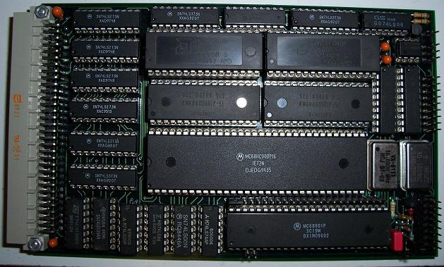
Incidentally, I still do my schematics by hand, since there are things about all of the schematic CADs that I don't like. At my last job, I got very proficient at OrCAD for schematic capture, but it was terrible. Now I go straight from hand-drawn schematics to PCB CAD, without using netlists & rat's nesting, etc.. And using this method of checking, I don't get any errors either. (While we're on the subject of schematics, let me challenge you to draw real schematics (like at the top of the potpourri page, rather than just a netlist written around boxes!) To give an example of the extreme density I've done with thru-hole (we do mostly SMT now though), see this portion of a mostly-analog PC board, first with U5 in the top-left corner missing (to show all the parts that go under the IC), and then with it installed. I put up to 11 resistors and diodes under each 14-pin IC, staggered in five rows:
The maximum density I've gotten with thru-hole, as an across-the-board average (IOW, big parts pulling the average down), was 45 parts per square inch. The most populous thru-hole analog board I ever laid out was the main board of the aircraft intercom shown near the bottom of the "Address Decoding" section, which had about 500 parts on a 3.8"x4.8" 12-layer PCB. (I did that one with a DOS-based CAD on a 16MHz '286 with 1MB of RAM, and it didn't need all the RAM to do it either!)
There are various online tools at https://www.eeweb.com/ for helping
determine things like trace width, wire inductance, transmission-line impedance, microstrip crosstalk, etc..
Off-Topic: Breadboarding Analog Circuits
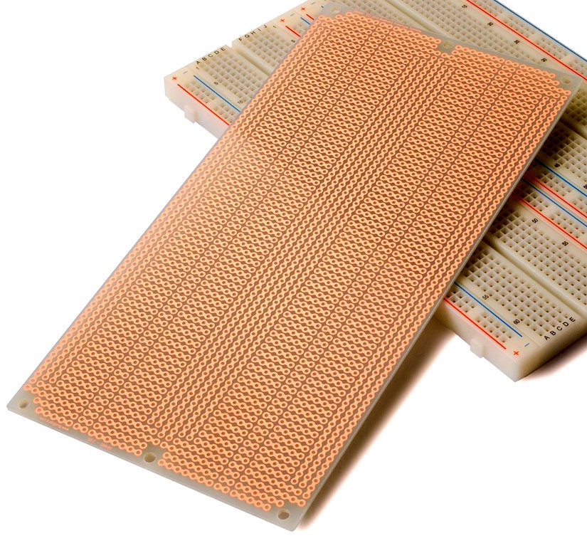
This is off the topic of making the computer itself, but I have used dozens of the Radio Shack 276-170 analog prototyping PC boards which have the same pattern that the common solderless breadboards with the hundreds of plug-in contacts have.
Unfortunately in the spring of 2017, Radio Shack closed their retail stores (see a
related forum topic). They
continued selling online though, and other companies sell virtually identical prototyping boards. Edit, Jan 2025: I see
they have apparently dropped all the prototyping products. Jameco has a
lot of the BPS models like what's show below though.
A similar one but with more buses plus holes at the ends for connectors, are several of BusBoard Prototype Systems' soldered breadboards shown here. Here's one of them:
You can download their .pdf catalog from the front page of their website. Jameco
is one of of their distributors. Go to their site and put "BusBoard Prototype Systems" in the search box.
wire-wrap Q&A <—Previous | Next—> I/O ICs
last updated Jan 19, 2025