home |
primer index |
1. Intro: Why 6502? |
2. addr decode |
3. mem map req.s |
4. IRQ/NMI conx |
5. 74 families & timing |
6. clk gen |
7. RST |
8. mystery pins |
9. AC performance construction |
10. exp bus & interfaces |
11. get more on a board |
12. WW Q&A |
13. custom PCBs |
14. I/O ICs |
15. displays |
16. getting 65xx parts |
17. project steps |
18. program-writing |
19. debugging |
20. pgm tips |
21. workbench equip |
22. circuit potpourri
6502 PRIMER: Building your own 6502 computer
Construction: Avoiding AC-Performance Problems
All links verified or updated 9/9/25.
#1: Yes, number one! Avoid plug-in (solderless) breadboards for this kind of
work! These are the worst of all worlds for computer performance, and it can bite you even at very low
frequencies if you have fast parts, because the problem is not the MHz but rather how fast an output slews from one
logic state to the other, measured in nanoseconds (ns). Solderless breadboards make for the longest connecting wires of
any method (meaning most inductance), have extra capacitance between neighboring tie points, and there's no chance of getting
anything even remotely resembling a ground plane. (And no, a piece of sheet metal underneath, connected to ground, does
not qualify. Not at all!) That's not to say you must have a ground plane. (Keep reading...)
Further, I'm not just talking about the connection problems of the Chinese solderless breadboards that use the wrong material
and shape of prongs inside. I only use the American ones with a lifetime warranty, and have never had a connection
problem with them; but I don't use them for making digital computers. I learned in the mid-1990's that they're not even
suitable for switching power supplies at 170kHz, because the high δi/δt, ie, the rate of change of current versus
time, makes for an extremely poorly behaved regulator. The only thing I use solderless breadboards for is analog and
control circuitry where the edge rates are low.
Unfortunately people insist on using solderless breadboards for computer construction, and we frequently find the resulting
problems reported on the forum with pleas for help to figure it out, when the builder has the connections right but the solderless
breadboards' stray inductance and capacitance are keeping his circuit from working. It causes so much grief, yet the builder
has a hard time believing that that's the problem!
If you really must use solderless breadboards, then at least put a lot of extra power and ground wires across
from one breadboard to its neighboring ones, not just at the ends but divide the length of the breadboard into three or four, and
put wires at the divisions, to shorten the ground return paths for the various signals. A major cause of problems is
connecting them like a neighborhood of cul-de-sacs:

If the resident of the house at the end of the cul-de-sac below the middle of the picture wants to give back a tool borrowed from
the neighbor right behind him on the next street and had to take the streets rather than just hand it over the fence, it'd be a long
route. On breadboards whose power and grounds are only connected at the ends, the loop area enclosed by that long path must be
charged up with an electromagnetic field, and that takes energy and time, and with capacitive effects it will set up more ringing and
groundbounce, and it will also have unwanted effects from coupling into other wires too. (Keep in mind that the wires really
only direct the energy rather than carrying it.) A grid of "streets" works better.
Jeff Laughton (forum
name "Dr Jefyll") applies this to solderless breadboards in a post
here. He starts the post with this important
statement: "It's best to avoid thinking of the Power & Ground Distribution network as something for connecting the chips to the
power supply. Where high frequencies are concerned [ie, the slew rates, not the clock rate! —GW], its
real job is to connect the chips to one another."
Keeping the connections short makes a big difference. In
this post, forum member "tmr4" shows pictures of two
solderless breadboard layouts he did, having done the second one much more compact after the first one was giving him trouble at higher
speeds, and says the second one worked at 10MHz whereas the first only only got to 2MHz. Similarly, in this post, forum member
"adrianhudson" writes, "I read somewhere, Garth's primer I think, about ground return paths on breadboard. I put several more
power and ground connections between my breadboards and bingo, fixed." Then in
this post, forum member "Paganini" writes, "I rebuilt
the keyboard circuit *yet again* on a different type of protoboard, using a ground return scheme like the one Garth described
earlier. This did the trick, and not only is it working great, it's working with the 74AHCT logic, so Blue April is back
to running at 8Mhz! Wheeee!"
#2: Do not run the processor's own buses off the board (as for an expansion bus) unless
you plan to never go over a couple of MHz. This is expanded on in the next section, Expansion Buses
and Interfaces. (This forum topic,
also mentioned elsewhere here, discusses getting good high-speed performance, and, on page 2, taking advantage of synchronous serial
interfaces as much as possible.)
#3: An actual custom PC board is best, preferably a multilayer with a ground plane.
(And no, pours & fills don't qualify—they're pretty worthless for this kind of work, unless they supplement real planes
and are done correctly. If they're not done correctly, they can actually make things worse).
This section could be huge; but I'll just refer you to the links at the bottom of this page, and here only make this comment
about VDD trace width, since someone just asked me about it. For cost-sensitive situations where someone feels
limited to a 2-layer board, I frequently see recommendations to make the power traces super wide. This has been very much
overemphasized and misunderstood. It's hard to get the myths to die though. Resistance is not the problem, and an
.008"-wide (0.2mm) trace can handle 500mA with ease. The real enemy is inductance, and making a trace wider on a 2-layer
board with no ground plane has very little effect on its inductance. Doubling the width of a 2"-long trace on 1oz copper, from
.010" to .020", only brings the inductance down about 10%, according to
this flat-wire (trace) inductance
calculator. IOW, it has almost no effect. Wanna go wider? If we widen it from .010" to .050", ie, multiplying
the width by five, the reduction in inductance is not even 25%. Bypass capacitors at each IC will reduce the need to
minimize VDD trace inductance anyway, and the ground connections will handle much of the signals' return currents.
So if you're limited to two layers, route a fine grid of ground connections, so there's the least impedance from the ground pin of
any one IC to the ground pin of another IC, then get the bypass capacitors connected with the shortest practicable connections from
each IC's VDD pin to its ground pin (which might mean putting them on the back of the board, under the IC). Then
route all the signals, and then sew-in a VDD grid with the room that's left. An autorouter won't have the
intelligence to do a very good job at that; so I would do the ground and VDD connections by hand.
I should address power planes next, because they're usually not done right. Do see the many links at the bottom of this page
though.
#4: If you have to route signals through a connector, do not put all the ground pins
at the ends! Have several power and ground connections, and distribute them somewhat evenly among the other signals, such that
no signal pin is very far from a ground or bypassed power pin. (I like to also arrange them such the if a card or module gets
plugged in backwards, the power and ground will still be correct and the risk of damage is greatly reduced.)
This video, long but good, makes the point that the signal
energy does not travel in the copper, but rather in the dielectric space between the signal conductor and the return current
path, that the copper merely guides it, and you want to minimize the area between a signal line and its intended return path
which is a ground or bypassed power pin, so there's less space to have to charge up. Here's a hypothetical example of 44 pins:
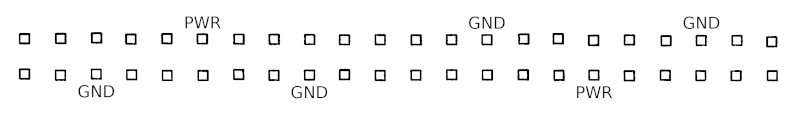
The power pins should be bypassed to ground at the connectors, both male and female. Here, no signal pin is more than 0.2"
away from a ground or bypassed power pin (assuming the pins are on a .100" grid).
#5: If you cannot do a custom PCB, use wire-wrap. Admittedly, wire wrap (WW) supplies have become
more expensive since I originally wrote this (as they've lost the economy of scale); but WW gives good density and lets you get parts
close together so the connections are short and relatively straight, improving AC performance. Forum member adrianhudson shows
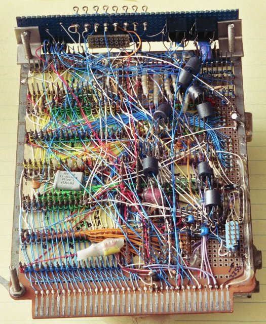
his board with minimal-length wires here. Here
is the bottom of my primary workbench computer:
and of a small Commodore 64 expansion board I made in 1997:
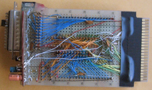
These don't have any plane (and from the oscilloscope displays of waveforms with lots of ringing, the larger, faster board above
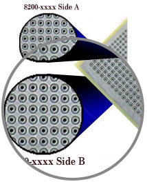
could sure use one), but it would be all the better if you have at least a ground plane, which you can get inexpensively with
protoboard like Twin Industries' 8100-series boards (see
this page and click on "8100 Series Plated
Through Holes - Single Power/Ground Plane," if not also a Vcc (or VDD—same thing) plane (ie, a power plane) which
you can get inexpensively with their 8200-series boards (see the same page, and click on "8200 Series Plated Through Holes - Dual
Power/Ground Plane"), shown here:
To make the ground plane work for you to best advantage, before you start wire-wrapping an IC socket, connect the ground pin(s)
to the ground plane immediately around it by soldering a tiny piece of wire, or a tiny washer if you can get the right size (I
think Vector used to sell them), from the base of the pin to the plane around it so the total hop is less than 1/16". Having
longer pieces of wire to make it easier will partly defeat the purpose.
Then with only one plane, you can bypass the power pins to ground without leads adding inductance, by soldering a surface-mount
capacitor from the base of the pin to the ground plane, as in this picture which I took without soldering, only positioning it to
show the idea:
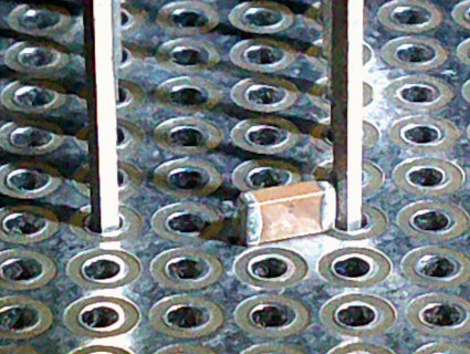
This is a 1206 size which is pretty big as SMT chip capacitors go, to make it easier to solder by hand. I stood it on its
long edge to try to keep the corners of the Vcc end from touching the ground plane; but a little of the plane might still need to
be cut away there with an X-Acto knife, unless you want to go for a smaller capacitor size, an 0805 or 0603.
...and now for those who are really dedicated :)
You could go for a power plane (on the component side of the board) in addition to the ground plane (on the wire side
of the board). It gets a little trickier. For best performance, put a strand of wire through the hole before putting
the socket in, and solder the strand to the power plane without getting solder in the hole itself. The strand needs to be
small enough that the socket pin will still fit in the hole with it. After the socket is in, you can cut the strand short
on the wire side (but don't cut the pin!) and solder the strand and pin to the hole's pad and thru-plating, filling the hole with
solder. Keep the solder off the upper part of the pin in case you ever need to wire-wrap it later. Check for shorts
after each one you do, so that if you do find a short, you know it's the one you just did.
Next, add the wires that distribute the clock signal, before you do the other wires, so that you can make the clock-distribution
wires lie flat against the ground plane, rather than elevated somewhat.
You may be asking, "So what's this about groundbounce and other potential problems? Do I need to worry about it?"
I see a lot of ringing and groundbounce on the oscilloscope with my home-made computers so I know it doesn't take 50 or 100MHz to
run into trouble. What I get is pretty astonishing, and I don't think the rise and fall times could get much faster without
bringing orderly operation to a halt. Note that rise and fall times do come before actual clock frequencies in this regard. Jack
Ganssle's YouTube video, "I Only Probed the Board With a Scope - Why
Did My Board Crash?," the part from about 2:20 to 3:00, graphically shows on a high-end oscilloscope that the ugly ringing remains
unaffected as he turns the clock frequency up and down.
When I built the one shown above, I did not yet know as much about high-speed digital (or what might be "high-speed" for this type of
construction), even though I worked in the mid 1980's in applications engineering at a company that made UHF and VHF power
transistors. (I also initially used slower parts and a lower clock speed on the workbench computer.) My next, faster one, if
not on a multilayer PCB, will be built with PLCCs instead of DIPs, on perfboard with power and ground planes and thru-plated holes. See
the list of links below for explanations.
Reduce your home-made computer's chances of trouble by keeping the parts close together and the wires as short as possible. Put
IC sockets right up against each other with almost no room between them. For home construction, go for a board no more than 6"
(15cm) square (at least the part that is used for the processor's immediate buses).
If you don't have a ground plane, make the finest grid of power and ground
connections that you practically can. Also put a capacitor in the range of .01µF to 0.1µF across each IC at the power
and ground pins with leads as short as possible. It should be monolithic ceramic or multilayer ceramic. Things like
the temperature coefficient won't really matter for this application. The power-entry point will have such capacitors from
VDD to ground as well as a tantalum, or better yet, an OS-CON capacitor. OS-CON capacitors' high-frequency impedance
is much, much lower than electrolytics'—even lower than tantalums'. OS-CON (Organic SemiCONductive electrolyte) is a capacitor
type made by Sanyo and a couple of other companies.
If you later want to get into higher speeds, I strongly recommend this
sticky forum topic ("Techniques for reliable high-speed digital circuits") for the why's and how-to's, with a load of links. Additionally,
and partly included there:
Note 5/4/19: The Fairchild ap. notes went offline after ON Semi took over Fairchild; but I requested that they put them back
up, and they did so and sent me the new links, which are below.
- PCB-design questions answered (forum topic)
- ground-plane question answered (forum topic)
- How long can my signal lines be before I need terminations? (answered in
this forum post)
- ground bounce & decoupling (Fairchild ap note, .pdf)
- dynamic thresholds & noise margins, which ground bounce
is involved in (Fairchild ap note, .pdf)
- terminations for Advanced CMOS (74AC & 74ACT) logic
(Fairchild ap note, .pdf)
- transmission-line effects (Fairchild ap note, .pdf) The
newbie may think ground is ground is ground, and you may not intentionally have any RF transmission lines; but if you build with
fast logic on a big layout with long wires especially with no ground plane, this stuff can bite you. 40 years ago
some people in the electronics field went into digital thinking it would be simpler mathwise and they'd avoid some of the analog
complications. But as digital got faster, it gradually turned into the worst form of analog—RF!
- A video, long but good, makes the point that the signal energy does
not travel in the copper, but rather in the dielectric space between the conductor and the return path. The copper merely guides it.
- Vcc capacitors (forum topic) (The idea
"ground is ground is ground" is incorrect. For the explanation and the easier way to get around it, see this one.)
- See why bypass capacitors can only do so much, and cannot
make up for poor construction (forum post). Forum member "Alarm Siren" replied, "You already managed to make it about a billion times
clearer than any of my university lecturers."
- excellent graphic animated
illustration of the value of putting bypass cap.s close to the chip they are associated with, with minimum inductance. It's
really about electrical noise radiated by the circuit; but the same thing affects signal integrity. (Last I checked, it was very slow
to load; so just be patient.)
- wire inductance calculator on EEWeb. Note
that even a simple piece of wire in free space has significant inductance. This online inductance calculator lets you compare the
inductance under different conditions. Note that increasing the wire's diameter has very little effect on its inductance!
- calculate inductance of a trace without a
ground plane. (The real enemy is inductance, not resistance, and here's a spoiler: Making a trace a lot wider has very
little effect on inductance.)
- Dr. Howard Johnson, industry guru on high-speed digital design, has a lot of great articles
here
If you want to go further in understanding the matter of PCB transmission lines, layering, the importance of the return current's path, etc.,
here are some more videos I came across. They're long, but helpful.
(and of course after you've watched one or more, you'll get suggestions for related videos down the right side of your screen.)
mystery pins <--Previous | Next--> expansion buses & interfaces
last updated Sep 9, 2025