All links below have been verified or fixed Dec 12, 2020.
Note that there are many ways to do most of these things, and probably just as many that a newcomer might think of that are DOA
for various reasons. The goal of this page is to make your home-made computer a useful "Swiss army knife" of the workbench, rather
than just a novelty for fun only, or a consumer item. There's no OS or kernel for it on my website yet, but I hope to publish my
6502 and 65816 Forths as time allows.
On this page:
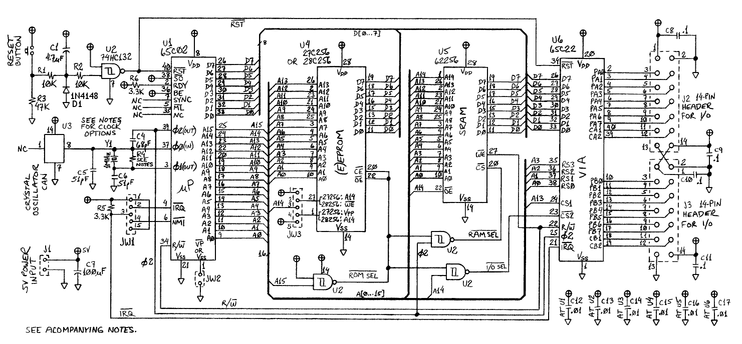
In the tips below, you will see that you can interface an unexpectedly high amount of things on a single VIA; but again, I strongly recommend at least one additional VIA for most uses of the computer. Note #9 above tells how to add more. Even if you don't want to add it to start, if there's any possibility at all that you'll want it in the future, at least leave room for it and the connectors.
Do get cozy with the VIA's registers, timers, and capabilities. Its name, Versatile Interface Adapter, is quite
appropriate. If you have questions, you can email me at wilsonminesBdslextremeBcom (replacing the B's with @ and
.) or post them to the 6502.org forum.
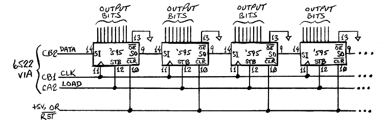
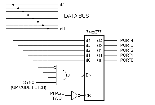
The 65(c)22 VIA's shift register (SR) has many modes of operation and uses. When speed doesn't need to be superfast (as when controlling relays, audio connections, the output voltage of a programmable power supply, etc.), you can use the SR to expand the number of input and/or output bits, virtually without limit. It becomes extra helpful when those bits need to be at a different logic voltage (like 12V), something other than the voltage the computer runs at. (More on that later.) First, consider a way to give lots of output bits at the computer's own logic voltage levels:
Although four 74HC595's (giving 32 output bits) are shown, you can expand the chain almost indefinitely, as long as the 595's are CMOS (ie,
have high-impedance inputs, unlike 74LS or other non-CMOS). CA2 is shown as the output to
latch the shifted values into the 595's, but you could use any output bit for that. I like to use CA2 to leave PA and PB free for other
uses where you might want all 8 bits of a port, like for an 8-bit A/D or D/A converter. (I'll address that further down
too.) Use 6522 SR mode 101 to clock the data out under control of T2, or mode 110 to clock it at half the Φ2 rate. Example
code is given about 80% of the way down the front page of the
16-Bit Fixed-Point/Scaled-Integer Math section. There's more there than you need for output only, but it shouldn't be hard to figure
out. I want to put code on this page here when I figure out how to put scrollable windows in it so the code doesn't make the page so long.
Similar to the above, the 65(c)22 VIA's shift register can be used to expand the number of input bits, again virtually without limit. For this, use SR mode 001 to clock the data in under control of T2, or mode 010 to clock it at half the Φ2 rate. These are bits 4, 3, and 2 of the VIA's auxiliary control register, or ACR.
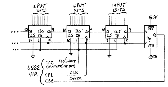
(The '165 signal pin not shown is the inverted serial output, pin 7.)
Althought only three 74HC165's (giving 24 input bits) are shown, you can expand the chain almost indefinitely, as long as the 165's are CMOS (ie, have high-impedance inputs, unlike 74LS or other non-CMOS). CA2 is shown as the output to load the 165's when it's low and allow them to shift the loaded data bits when it's high. (Later, when we address using the same SR for both and input chain and an output chain, we will need a 74HC126, and the CA2-high output will then also enable the '126.) Again, I like to use CA2 to leave PA and PB free for other uses where you might want all 8 bits of a port.
"So why the 74HC74 D-type flip-flop at the end of the chain?" you might be asking. The answer is that the VIA looks at the data line at the first rising Φ2 clock edge after the serial clock goes up; but the '165 also goes to the next bit when the serial clock goes up, so the first bit the VIA sees is bit 6, not bit 7. Since the '165 chain gets ahead by one bit, we delay it by one bit with the flip-flop. There are other ways to get around this, like putting the output of the last '165 around to the input of the first one and rotating in software (which is not practical if the chain spans multiple circuit boards), or offsetting the bits in the hardware connections (which might require adding an extra '165 to every board if the chain spans multiple boards).
When we get to the software, note that after you latch the data into the 165's, you have to do a dummy read of the VIA's SR to start the
shifting process. Then allow enough time to finish the process before reading again—at least 16 Φ2 clocks in mode 010, or longer
in mode 001, depending on what you have T2 set to. Read once more for each additional '165. To restart the process and get a new
set of readings, put CA2 low to load the new set of data into all the 165's, and then put it back high again to shift, then begin the shifting
again, starting with the dummy read.
The circuit at approximately the middle of the front page of
the 16-bit scaled-integer math section gives the idea for combining the two uses above. The circuit there is a last-resort method
to interface to the huge math look-up tables in ROM if all your other I/O is taken. Interfacing to huge memory this way is slow, but still
much faster than actually calculating the various trigonometric, logarithmic, and other functions, and it's accurate to all 16 bits.
Some situations require interfacing to control circuitry that works on 12V or other voltage substancially higher than the 5V (or 3.3V, or whatever your creation works at). I have, many times, used for example 4066, 4051, 4052, and 4053 analog switches to control 12V analog circuits (mostly audio), and these ICs needed the higher-voltage logic. (Maxim has these available with 5V logic control, but it's a very expensive way to go.) Consider the common and cheap 14-pin LM339. This diagram shows going from TTL-level logic to 12V logic levels:
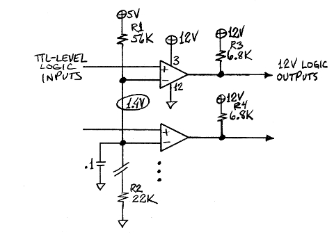
If you take the top of R1 to a different voltage, you will need to change the resistor value. If this goes to a separate board that only has
12V (or other high voltage) available and not 5V, you can of course take R1 to that voltage, and calculate the adjusted value. 1.4V
across 22K gives 63.6µA, so take your high voltage minus 1.4V and divide that result by 63.6µA to get your resistor
value. It's not critical to get the reference voltage very exact in this case, so you can round to the nearest standard value within
20% or so and do just fine. The input bias current of each LM339 section is typically only 25nA, not enough to make a dent in the
calculation, so we can leave it out for simplicity's sake, even if you run the same reference to many LM339 sections.
For going the other direction, ie, higher voltage to 5V logic, you can do something like this:
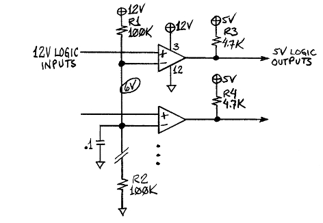
It does not have to be 12V of course. The LM339 can work up to 36V, and although its power supply voltage needs to be at least 2V,
the input & output can go even much lower than that. If 12V (or similar) logic is driving the input, you will do just fine if you
want to connect the reference to the 5V supply, and then you won't need to get the reference from resistors.
A comparator is similar to an op amp, but it's not an op amp. The comparator is made to have its output hit the rails and recover more quickly than an op amp of similar price can. The penalty is that the phase response is not kept under control to keep it stable in an analog output range; but that's not what it's for anyway. One of the reasons for this comparator however is the open-collector output that lets the high output voltage be independent of the comparator's supply voltage.
For best speed:
For going between 5V and 3.3V or other low logic voltages, there are other ICs on the market that would be more suitable
than the 339 (although I have used the 339 there too), like the 74LVCxx family. Additionally, after I wrote the above, "ttlworks" on
the forum alerted me to the 74LS06 (inverting) and 74LS07 (non-inverting) open-collector hex buffers which
are much faster than the 339 and have a maximum output voltage of 30V but whose inputs do make for a greater load and are not available in
CMOS; and Jeff Laughton alerted us to
this series of TI videos
on their LSF family of voltage-level translation ICs.
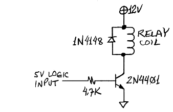
The resistor value was chosen for a 15mA coil and making sure the transistor is really saturated even if its gain is at the low extreme of
its allowable current-gain range and the circuit feeding it can't pull up to more than about 3V. CMOS will be able to pull it up
higher but the overdrive is nowhere near enough to hurt anything.
If you need a lot of these, you might do better to use an IC like the
ULN2803
which has 8 Darlington drivers in an 18-pin package with integral resistors and protection diodes. That would replace 24 discrete
components, three for each circuit above, times eight. The only negative about it is that being Darlington, the output voltage
won't come down to much under a volt. The configuration shown above however allows the output voltage to come nearly all the way
to ground if the load is light enough and the bias current strong enough for the chosen transistor.
In the automated test equipment I designed, built, and programmed in approximately 1990, I drove approximately 75 relays by way of Allegro Microsystems UCN5821A (I think it was made by Sprague at the time) 8-bit, serial-in, parallel-out 16-pin shift registers which are rated for 50V, 350mA, made specifically for driving relays and other heavyish loads. It looks like Micrel, now acquired by Microchip, sells it now under the part number MIC5821BN. These were mixed in with lots of 4094's in the same serial chain all controlled by the same three pins of the 6522 VIA.
There's also TI's TPIC6 line of logic ICs, with for example the TPIC6A595 shift register that is similar to the 74HC595 mentioned above in the section "Using the 6522's shift
register for tons of output bits" but with open-drain outputs that can handle 50V when off and 350mA each when on, even though the IC's
power supply and logic inputs are 5V, and it has extra ground pins to handle all that extra current (IOW, it cannot be used as a drop-in
replacement for the 74HC595). Also available are the '259
8-bit addressable latch and the '273 octal D-type latch,
although these last two are much more expensive, at over $4 each in singles.
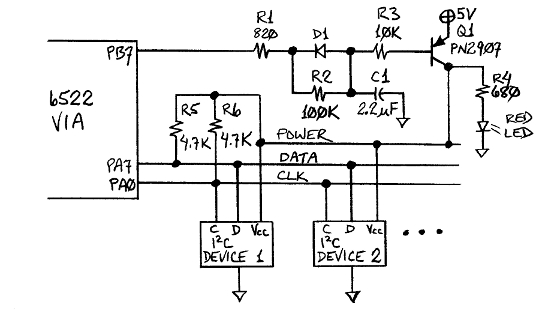
You can use any I/O bits you want, but I chose the ones above for particular reasons.
Next you might be wondering about the pull-up resistors. This is how I²C manages to send signals in both directions without bus contention. Devices can only pull it down, not up. I've done it such that the master does pull the clock line (but not the data line) both up and down, and that's normally not a problem; but the spec does allow multiple masters, and also a few devices can hold the clock low to tell the master not to send the next bit yet (which would require that the master check that the clock line has floated up before it pulls it back down). Handshaking is usually accomplished through the ACKnowledge bit though, and that's on the data line at the end of a byte.
Ok, so how do you have the VIA only pull down and not up? Simple—store a "0" in the applicable bit of the output register, then write to the data-direction register (DDRA or DDRB) for the particular port. When you want it to pull it down, you set the bit to be an output; or to let the pull-up resistor pull it up, you set it as an input, even if you don't particularly need to read it. (The interesting thing about that is that since a "1" in the data-direction register bit means "output" and a "0" means "input", pulling it down requires setting it to "1", and letting it float up means setting it to "0", instead of vice-versa.) You don't actually keep writing to the output register itself. This is one place where the 6522 is far more efficient codewise than the 6521 or 6520 which do not allow a light-footed method of quickly going from accessing the ports to accessing the data-direction registers and vice-versa.
The I²C devices are all connected in parallel. Each class of device has an address group assigned to a few bits in the address byte, and then the device might also have a few extra pins that you can connect to Vcc or ground to provide more bits in the address byte and allow several devices of the same class to be on the bus at the same time. This way you can have more than one EEPROM, more than one digital thermometer, more than one D/A converter, etc..
If you want to make module to plug in, I would suggest the I2C-6 connector standard we devised on the 6502.org forum. The page has diagrams and photos. Use of the interrupt pin is optional, but it would be good if you incorporated it on your computer so that for example if you make a module for time and date and it has an alarm capability which uses the interrupt, or a keypad controller that interrupts when a key is pressed, you're all set. I offer a tiny I2C-6 32KB 24256 EEPROM module on the front page of my site.
There is 65c02 assembly generic I²C code here. Various devices will have their
own detailed operation which will be given in their data sheets; but there will be basic things that they all share. The link
also has Forth and PIC code for 24xx I²C EEPROMs, and Forth code for the MAX520 I²C quad 8-bit D/A converter.
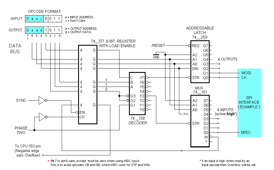
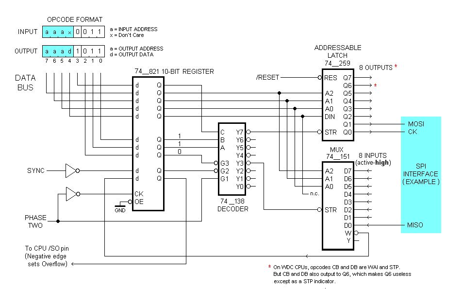
Wikipedia has quite a write-up on SPI. Unlike I²C, SPI can be full duplex; and because it is not limited by passive pull-ups like I²C is, SPI's maximum speeds are dozens of times as fast as I²C's. For this reason, the larger flash memories especially will be found in SPI and not I²C, as storing a 10-megapixel photograph for example to an I²C memory would take much too long. Bit-banging with a 6522 VIA as shown below will not operate SPI anywhere near its maximum speed, but it still enables us to help ourselves to hundreds (if not thousands) of great ICs on the market, made by dozens of manufacturers. (For maximum SPI speed available in a 65-family IC, see the 65SPI (not to be confused with 65SIB) I/O IC which is designed and sold by Daryl Rictor and provides direct and complete SPI support in a 65-family IC, without bit-banging.) Jeff Laughton's circuit tricks much further down this page also make possible much faster bit-banging, using illegal 65c02 op codes. For example, you can set or clear an output bit in a single clock cycle without affecting the other bits in the port! Not quite as fast as Jeff's, but more efficient than using a VIA, is the bit-I/O module I offer on the front page of this site, starting Aug 17, 2022.
SPI normally involves four wires for one SPI device (or slave), plus an extra one for each additional device. There's a clock line (often abbreviated SCLK for "serial clock"), a master-in, slave-out (MISO) data line, a master-out, slave-in (MOSI) data line, plus one negative-logic chip-select (CS) for each device or slave.
Each transaction is begun by putting the slave's CS line low and then sending the command, ie, telling the slave what you want it to do, whether to take the following data and do something with it, or output some data, etc.. Non-selected devices stand by and don't respond to anything on the clock, MISO, or MOSI lines. The SPI modes used by the different slaves on the bus do not need to match, as only one slave will be enabled at a time (unless you daisychain, something which will not be addressed here.)
As long as you don't exceed the device's speed limits (which you're not likely to do if you bit-bang with a 6522 VIA), there are no particular timing requirements like RS-232 has, so bit-banging it is very easy. More on that later. Here's a really basic SPI connection:
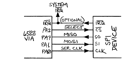
You can use any I/O bits you want, but I chose the ones above because again bit 0 of a port is the easiest and quickest to pulse in software (using INC and DEC), and bit 6 or 7 of a port are easiest to test (using the BIT instruction).
The arrows show signal direction. Since normally no line is bi-directional, it makes it easy to convert logic voltage levels if necessary.
It wouldn't be a bad idea to put weak pull-up resistors on all the lines so that no line floats between logic levels before the VIA is set up. Non-WDC VIAs (like Rockwell, even the CMOS ones) do effectively have a pull-up resistor similar to 74LS, but WDC's are truly high-impedance CMOS in the input mode. However, at least an accidentally selected SPI slave won't do anything if the clock and MOSI lines don't toggle in a sequence that it understands as a valid command.
Depending on the SPI modes you need, you can sometimes share clock and data lines with I²C. You'll have to observe the following:
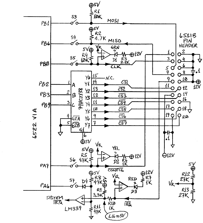
To interface to more devices, you will need more CS lines, using more VIA output bits. This is shown below, along with the entire 65SIB (6502.org Serial Interface Bus) circuit on my workbench computer. 65SIB is basically SPI but expanded in several directions at once, making it suitable as an external bus too, and accommodating devices ranging from dumb to highly intelligent. (Don't be scared off by the complexity of the circuit. Half of it is just to feed the annunciator LEDs.)
Notes:
We also have the SPI-10 connector standard for small modules, similar to I2C-6 above. See the spec here. I have a tiny SPI-10 flash memory module available on the front page of this site.
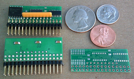
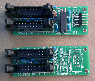
When I built my first 65SIB device on a proto board (not a PCB), I found that it was quite a bit of work to wire up the connectors
and the voltage-translation circuits; so later I laid out a PCB for future projects, and am making it available to others as well,
on the front page of this site. It looks like this (shown in two stuffing versions):
10/11/23: Forum member BruceRMcF just posted
a couple of ideas for using the VIA to do SPI somewhat faster than normal bit-banging.
Starting at the simplest point, you can have a pushbutton switch from one of an I/O IC's input pins to ground, and a resistor of 4.7K or 10K to pull the pin up to Vcc when the button is not being pushed. Note that as long as you're not needing to push the button, you can use this pin for something else too. When I've designed products with PIC microcontrollers which are programmed with a serial connection with one line for clock and one for data, I've put pushbuttons on the same pins, as there will never be a need to push a button while the device is being programmed, and the programmer will never be connected when a button needs to be pushed.
Going to the next step, you can have several buttons connected to output bits, with a common connection to a pulled-up input bit, like this:
Note that the output bits can be connected to other things as well. Just don't press more than one key at a time if you keep the bits in output mode full time, or you'll have two or more outputs shorted together, unless you put a diode (preferably a Schottky one) above each key switch, with the cathode at the top. (There's another way to get around that, discussed in a minute.)
I'm partly out to get maximum function with minimum parts though, as construction takes time, and hardware is a bigger job to swap out or modify than software is.
Your software needs to bring one of the output lines down at a time, then read the input line and see if it's high or low. A high input bit means the key that is on the low output is not being pressed. Make the software cycle through them. More on software considerations in a minute.
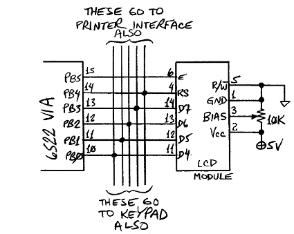
The five-key keypad is what I have on my workbench computer, and the five VIA output bits feeding the keys also go to the LCD and my printer interface. I do the software development on a DOS PC and send code over the RS-232 line; but the keypad is convenient for various things once a piece of code is set to running. The keys can be used for anything you determine in your software, but the functions I usually give mine are:
| Yes Enter Continue |
Up |
| No Cancel Exit |
Down |
| Help Menu Edit |
I have this to the right of the LCD on my 6"x4.5" workbench computer, with 6mm tactile keyswitches soldered to DIP headers that are plugged into DIP sockets; but as I gave it commands from the PC on the desk opposite the workbench and turn around toward the workbench to see instant results, there were times that I wanted the keys within reach without having to get up each time; so I also made a remote keypad and added a pin header on the workbench computer to connect it with a long cord, like this:
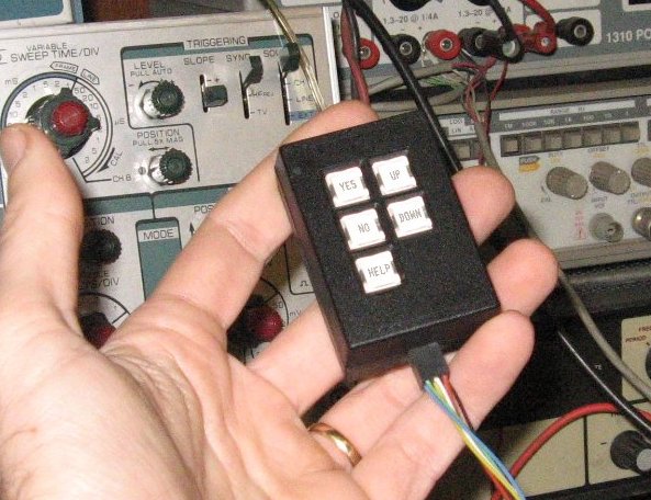
(This is in my Tip of the Day column too.) The connections to the two keypads are in parallel, so it all goes to the same I/O bits, and a given key has the same effect regardless of which keypad it is pressed on. The pin header it plugs into has a few extra pins so I could also put a duplicate LCD on the remote module.
For more keys, even a full keyboard, you can do something like the following. (To save drawing time, I'll just use a circle to represent each switch connecting the vertical line and the horizontal line that go through that circle.)
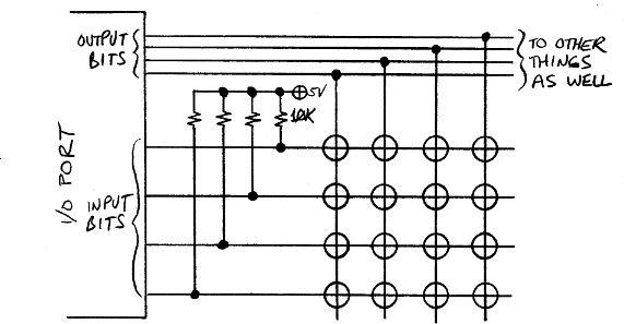
As above, pressing more than one key at a time could cause contention (depending on which ones they are), unless you add the diodes or other means to prevent shorting outputs to each other. The software needs to lower one output line at a time, then see if any of the input lines are low, then go to the next output line, cycling through the set. It might be best to have it return a pair of bytes with one bit to represent each of the 16 keys.
Actually, there is a no-diode way to prevent the shorting-outputs problem. You can write 0's to the output bits (by writing to the VIA's ORA or ORB), and then make only one of the output bits an output at any given time (by writing to the VIA's data-direction registers DDRA or DDRB). When it's not pulling the line down, any given bit is an input. This has the effect of an open-drain (or open-collector) output. We pulled this trick above in the section on interfacing to I²C, which has sample code linked. The only pullups then are passive, ie, the resistors—and BTW, it might then be a good idea to put pull-up resistors on those as well, not just the inputs, so there won't be ambiguous logic levels at any pins when keys aren't being pressed.
16 keys is what I put on the last automated test equipment setup I designed, built, and programmed at my last place of work in about 1990:
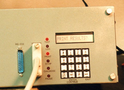
An earlier set I did used a full PC keyboard, and it just took a lot of space on the workbench, and it, plus the big monitor, turned out to somehow make the test operator think she knew more than she did and it became a bit of a pain. The smaller keypad afforded ways to get to all the menu items and enter the needed info just fine. The blank key could be used for a shift key to give other ones more functions. These ½" square Grayhill type 87 keys are really nice because their pins fit into prototyping board and they have clear caps you can remove to put labels underneath. (As you can see, I didn't go to the effort to make the labels look really professional.)
You can get away with taking fewer bits on the 6522 VIA (or other I/O IC) if you use something like a 74HC138 3-to-8-line decoder. The above shows 16 keys on 8 I/O bits; but with the '138, you could put three 6522 outputs to the '138 and have the 8 outputs of the '138 feed 8 columns, then with only three inputs on the 6522, you could have 24 keys (3x8) with only 6 bits total on the 6522 instead of 8. You can take it further of course. A keypad is not a high-speed device by any means, and the serial I/O above, using 74HC165's and 74HC595's, can easily put an 8x8 (or bigger) key matrix on the 6522's shift-register port, along with lots of other things, and not take any additional pins on the 6522.
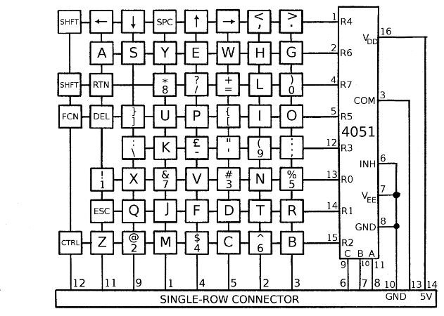
The 6502-based Oric computer keyboard used a 4051 instead of a 74HC138. Since it's a 1-to-8 analog switch (with three control bits), the non-selected outputs were high-impedance, so no other provision was necessary for allowing multiple keys to be pressed at once. 4000-series logic is very slow and not suitable for a lot of computer use, but you won't be making hundreds of thousands of keystrokes per second anyway. Here's the Oric keyboard schematic:
You must debounce! "What does 'debouncing' mean?", you might ask. Switches are not perfect, and if you look at the output as they make or break contact, it will not be a single, solid, fast edge, but a bunch of up-and-down for a few thousandths of a second until the switch quits bouncing and settles down. This was illustrated in the "Reset requirements" page, and it shows deboucing there in hardware because you cannot do it in software while you're resetting the processor. You have probably had the experience of a bad calculator or other keypad where it acted like you pressed a key many times even though you pressed it only once. The calculator probably had some debouncing, but not good enough for a less-than-new keypad. It's very irritating!
It is much easier to do debouncing in software than hardware. What I have done for debouncing on many products is to require that the switch be closed for at least 30ms at a time before it is recognized. It is sampled many times in that amount of time, and if any sample shows it released again, the count starts over. The same goes for releasing it. You may think that 30ms is unreasonably long; and indeed new switches won't need that long, but as the switch gets older, it will need increasing amounts of debounce time. (What I plan to do in the future is to register the keypress almost immediately, but not register the next one until the needed debounce time is met and it has clearly been released and pressed again.)
I frequently also add auto-repeat, and, on the workbench computer, I have a variable to set the delay before repeat begins, and another variable for repeat rate. Auto-repeat is useful even on a small keypad, because you might for example want to increment or decrement something with the up- and down-arrows while watching the results, and having sometimes even hundreds of button pushes (ie, no auto-repeat) would be tiresome, slow, and also reduce the life of the switches.
Newcomers tend to do the timing in software delay loops, but I would encourage use of a real-time clock (RTC) instead, whether it's an RTC chip with adequate time resolution, or a software RTC that is interrupt-driven by timer 1 (T1) of the 6522 VIA, or other method. My interrupts primer tells how to set up the RTC using the 6522, and has complete code, starting a little over half way down the page. (Enjoy my out-of-date cartoons!) Having an RTC allows the computer to be doing something useful between key repeats, and the repeat rate stays consistent regardless of the varying size of the job between repeats.
My article on simple methods to do multitasking without a multitasking OS has example code for doing keypad debouncing and handling a shift key plus auto repeat of the cursor keys, near the end, timing things while allowing the computer to be done other things at the same time.
Two-key rollover can be done in sofware too. Just stop scanning the keypad or keyboard until the currently pressed key is released. Until then, you only watch that one key.
For other keypad- & keyboard-interfacing possibilities, I should mention that there are many I²C keypad controllers on the market that have built-in debouncing and sometimes also drivers for 7-segment LEDs and other I/O built in, and you can connect them (along with other things) to your I²C interface described above. Note also that the common PS/2 keyboard interface is very similar to I²C. Daryl Rictor shows how to interface it to a 6522 here, with code, and shows how to do it with an AVR microcontroller here, again with code, and interface it to his 6502 SBCs. (Please note that the power pins on his are slightly different from what I put at the top of this page.)
The darnedest thing I've ever seen in keypad interfacing was to connect the key switches to an arrary of resistors pulled up
to Vcc and produce a single voltage to go into an A/D converter. The application was a microcontroller that was short on
I/O pins but had a spare A/D input!
NOTES:
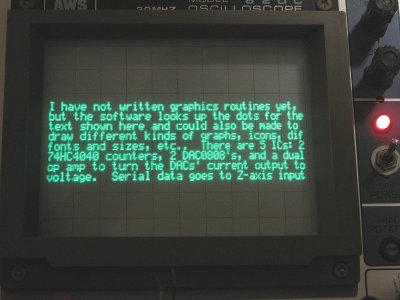
I have only a mild interest in graphics. I made a very simple circuit and software to do raster graphics on an analog oscilloscope. See http://forum.6502.org/viewtopic.php?p=15348#p15348.
I also have a small 128x64-dot graphics LCD that is interfaced by SPI, so I put it on the 65SIB. I have working sample code for it here. Here's a few seconds of demo video done for experiment purposes, using a random number generator to produce sets of 25 random segments then displaying the screen memory:
8/30/22 note: I just got a new Epson LX-350 to replace a couple of decades-old Epson printers here that were ailing. It was $217 brand new on eBay, no more than I was expecting to have to pay for a repair on the others. I'm very pleased with it. Print quality is excellent for a 9-pin, and it's faster than any I've seen before, maybe a little smaller too. It has parallel (which I use), RS-232, and USB interfaces. It's the cheapest of the fourteen (!) models of dot-matrix impact printers that Epson still offers. They have 24-pin ones too. They know that this market isn't going away, and they've picked up the slack where other manufacturers have stopped making them. Epson puts the same command set in all of them, the ESC/P printer control language, the industry standard for simple, sophisticated, efficient operation of dot-matrix printers, and you can download the command reference here (.pdf) (since this information was not in the manual).
The timing diagram from the manual for one of my several parallel printers shows:
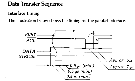
The lower two lines, data and strobe, are computer outputs to the printer, while the upper two, busy and acknowledge, are computer inputs from the printer. You do need to pay attention to the busy line, but I've never paid attention to the acknowledge line. Technically, the busy line is not an acknowledgement that the byte you just sent it was actually received; but this is the way I have done it since 1990, with a half-dozen different printers from four different manufacturers, and it has always worked flawlessly. the reason I started doing it this way was probably to save another VIA I/O bit. That additional line would have to be on one of the CA or CB lines for the edge-sensitivity since the ACK\ pulse is narrow enough that it might get missed if I only sampled it.
Since there's no hurry with printers and the occasional poll will stay ahead of the printing and keep data in the buffer anyway, I've never put them on interrupts. I might if I were spooling a super long printout, but I've never done more than a couple of pages at a time with the workbench computer and the automated test equipment at my last place of work; and in those cases, an interrupt-driven process could continue while the non-interrupt-driven print routine babysat the printer.
Your software needs to check the printer's status before every single byte. Before stopping with an error condition saying the printer is not ready, your software should allow a couple of seconds for the printer to say everything is ok. Especially in non-graphics mode, you will be able to send data much faster than the printer can print it, meaning you may fill up its buffer and have to wait for the printer to be ready to take more data.
Parallel printers normally have a 36-contact female Centronics connector, and for reasons unknown to me, computers with a parallel printer port usually have a female DB-25 connector on them, so the standard printer cables (before USB) are generally terminated in the male of each of these two connector connector types. I put a 16-pin header on my workbench computer since it takes so much less board space, then made up an adapter cable to go from IDC (to plug into the pin header) to DB-25 (to mate with the standard printer cable). The connections go this way:
| IDC pin |
DB-25 pin |
Centronics contact |
function (Note 1) | into or out of printer? |
Notes |
|---|---|---|---|---|---|
| 1 | 1 | 1 | strobe | IN | |
| 2 | 2 | 2 | D0 | IN | |
| 3 | 3 | 3 | D1 | IN | |
| 4 | 4 | 4 | D2 | IN | |
| 5 | 5 | 5 | D3 | IN | |
| 6 | 6 | 6 | D4 | IN | |
| 7 | 7 | 7 | D5 | IN | |
| 8 | 8 | 8 | D6 | IN | |
| 9 | 9 | 9 | D7 | IN | |
| 10 | 10 | 10 | ACK | OUT | 2 |
| 11 | 11 | 11 | Busy | OUT | |
| 12 | 12 | 12 | Paper out | OUT | 2 |
| 13 | 13 | 13 | -- | ||
| -- | 14 | 14 | auto feed | IN | 3 |
| 15 | 15 | 32 | Error | OUT | |
| 16 | 16 | 31 | init | IN | |
| -- | 17 | 36 | select | IN | 3 |
| 14 | 18 | 33 | twisted pair ret Gnd | ||
| 14 | 19 | 19 | twisted pair ret Gnd | ||
| 14 | 20 | 21 | twisted pair ret Gnd | ||
| 14 | 21 | 23 | twisted pair ret Gnd | ||
| 14 | 22 | 25 | twisted pair ret Gnd | ||
| 14 | 23 | 27 | twisted pair ret Gnd | ||
| 14 | 24 | 29 | twisted pair ret Gnd | ||
| 14 | 25 | 30 | twisted pair ret Gnd |
Note 1. Note the six negative-logic signals. (Their overbars are not very visible.)
Note 2. These pins on my workbench computer's IDC are not connected.
Note 3. I did not connect these, but they have DIP switches in the printer so external connection is not always necessary.
Columns 2 & 3 represent the standard parallel printer cable. Columns 1 & 2 represent a ribbon cable I made up, but you might want to just put a DB-25 on your computer board for the purpose.
From the other things on this page, you're probably getting the idea by now of how to connect this to a 6522 VIA or even through shift registers. (After all, a line printer is another thing that's not exactly fast. Putting it on the VIA's SR is not going to be a burden speedwise!) To get as many things on the first VIA on the workbench computer, I even have to split the eight bits of printer data between five bits of port A (shared with the LCD and keypad, as shown in the schematic in the display section above) and three bits of port B. (I know it sounds like a mess, but once the software for it is written, it just does its job and you forget all about it.)
I might post code later. All I have now is Forth code from various projects—not a single one in 6502 assembly.
STA VIA_PBThat's it. No separate .asm file for this one. (Just make sure you've put the port bits in output mode, by storing $FF to the data-direction register.) Here's the circuit:
Notes:
If you need more sharing of VIA ports, like to be able to use the same VIA bits to talk to something else without changing the DAC's output, you could add an 8-bit latch such as the 74HC373 or '374 and use just one extra bit from the VIA to trigger the latch after putting the desired bit pattern out the 8-bit port. The point of this particular DAC however is speed; so if you want to go with serial (which is much slower) to further extend the number of things the existing VIA pins can interface to, you might as well go with the I²C MAX520 or 521 discussed below which have 4 and 8 DACs and need virtually no support parts.
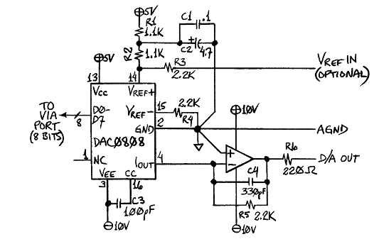
This DAC0808 BTW is the same converter I used on my analog oscilloscope raster graphics circuit to take the counters' outputs and drive the X and Y inputs of the oscilloscope.
In the automated test equipment
I designed, built, and programmed at my last job in about 1990, I used
DAC1220's which are nearly the same but
in 12-bit, in an 18-pin DIP. I used these to set power supply and other voltages and to control signal amplitudes. The
DAC1220 is apparently no longer made, but the AD7541A is nearly the same thing, somewhat improved.
The MAX520 quad I²C
8-bit DAC in 16-pin DIP I mentioned earlier needs virtually no external components, so there's really no circuit to
draw. There's simple Forth code to drive it about 2/3 of the way down the GENRLI2C.ASM
file which starts with general I²C-driver 6502 assembly code. I might recommend the MAX521 in 20-pin DIP instead though,
since it has 8 DACs instead of 4 and it has output buffer amps so it can drive a decent load without the output voltage drooping
seriously. The 520's outputs should only drive high-impedance loads.
For a super-simple 9-level D/A converter, remember you can use the VIA's SR data output as mentioned earlier:
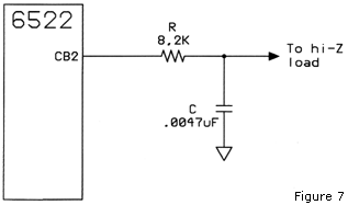
shown with a little more explanation at http://wilsonminesco.com/6502interrupts/index.html#3.3 in my interrupts primer (where this figure came
from). Driver code is too simple for a separate file, so here it is:
INIT_SR_DAC:
        LDA   #00010000B   ; Set SR to shift out free-running at
        STA   VIA_ACR      ; T2 rate.  (T2CH does not get used.)
        STZ   VIA_T2CL     ; Zero the T2 counter's low-byte latch for fastest
        RTS                ; possible shift rate, to make it the easiest to filter.
 ;------------------

_3BIT_TBL:                                     ; "DFB" in C32 is "DeFine Byte."
        DFB   00000000B, 00010000B, 00100010B  ; The point here is to distribute the bits
        DFB   01010010B, 10101010B, 10101101B  ; such that the toggling frequency is kept
        DFB   11011101B, 11101111B, 11111111B  ; as high as possible for easy filtering.

WR_SR_DAC:                 ; Start with number in the range of 0-9 (inclusive) in A.
        TAX                ; Skip the TAX if you already have the number in X.
        LDA   _3BIT_TBL,X  ; Get the distributed-bits pattern from the table,
        STA   VIA_SR       ; and write it to our make-shift D/A converter.
        RTS
 ;------------------
This is a Forth-to-assembly translation of code I used when I did DTMF output with this method. Worked
like a charm. Believe it or not, it worked quite well for speech too, if the dynamic range is really compressed. I
don't remember trying it for music, but I can't imagine it would be very enjoyable! Using a CMOS 6522 (65c22) will
make give a higher, more-consistent output voltage, since CMOS can pull all the way up to the 5V (unlike NMOS), and with a lower
impedance. The SR always finishes sending out a byte before starting the next, so you don't have to worry about glitches
from not timing the write just right. And again, this SR mode keeps shifting the same value out over and over,
free-running, until you write another one to it. It uses T2 to govern the shift rate, so T1 is left available to produce
interrupts for the sampling rate.
Notes:
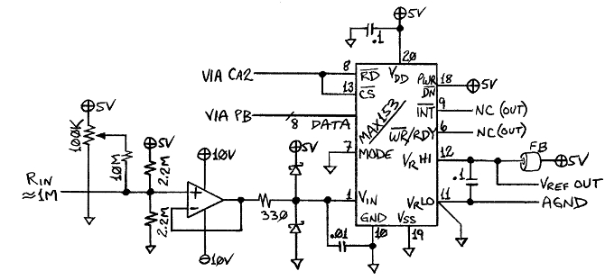
The code to set it up and to read it is:
INIT_AtoD: LDA   #00001110B
           TSB   VIA_PCR     ; Set CA2 high.  I put the CS\ of the A/D on CA2.
           STZ   VIA_DDRB    ; Make all bits of Port B to be inputs.
                             ; First reading after power-up is inaccurate, so get it out of the way, by continuing:
READ_AtoD: LDA   #00000010B  ; No entry requirements for READ_AtoD.  At end, A/D result is in Y.
           TRB   VIA_PCR     ; Set the CS\ of the A/D low.
           LDY   VIA_PB      ; Read the A/D result.  At 5MHz phase-2 clock freq, you'll need one NOP between TRB & LDY.
           TSB   VIA_PCR     ; Set the CS\ of the A/D back high.
           RTS
 ;-----------------------
What I have not shown above is the sockets for plug-in modules for anti-alias filters and other signal conditioning. (Depending on what you're doing, you may not initially have any need for that.) I have various places to connect to the outside world. I put 3.5mm plugs on the front panel which I can plug audio straight in, other projects have been plugged into the module sockets, and some went through the board-edge connector at the back. The monitor speaker amplifier can be switched between A/D input and D/A output, both post-anti-alias filters.
I originally had an ADC0820 in the circuit which is nearly pin-compatible, but later went to the faster MAX153. (I needed more NOPs with the ADC0820.) It required very minimal change to the circuit. Edit, 7/16/22: I was just shopping for more parts, and found that the MAX153 has gotten super expensive, like $24US! The ADC0820 is one-quarter to one-third the price. The MAX114 seems to be the same thing inside as the MAX153 but is about half the price and yet has four input channels. The MAX118 is the same thing for eight channels instead of four. I'm finding that all the fast A/D converters are expensive now. My purpose for the '153 is speed, and getting exact timing on the readings; so if you don't need the speed but you want more resolution, you you could use SPI or I²C A/D converters, perhaps putting them in SPI-10 or I2C-6 or 65SIB devices you plug into those ports on your computer.
For a home project I have not done yet, I piggy-backed a second MAX153 to get two in the space of one (but see my 7/16/22 update note above about the MAX114 which is a newer version, 4-channel and yet cheaper, and the MAX118 which is the 8-channel version):
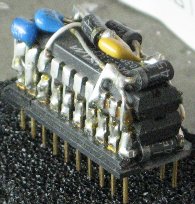
(BTW, you can see a lot of stacking of different ICs, sometimes to extremes, in the forum topic
"OT: stacked (DIP) chips.") My double MAX153
above only takes one extra VIA pin to interface it, for the second CS. The
data bits' connections are common.
With something like an I²C data converter, the exact time of the sample may be difficult to nail down accurately; but we would probably not be using that interface for a signal that changes quickly, let alone for audio. SPI is considerably faster; but the parallel converters here would offer much better timing for audio if we interface them to a 6502 with timing based on interrupts.
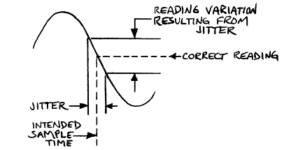
If the sytem clock (ie, Φ2) jitter and aperture jitter are negligible such that variations in interrupt latency make up basically the whole picture, the total RMS jitter for record-playback is the square root of the sum of the RMS record jitter squared and the playback jitter squared:

6502 instructions are mostly 2-6 cycles (7 is rare) and the average is 4. (Caveat: See the forum topic "A taken branch delays interrupt handling by one instruction.") Since all instructions take at least two cycles, an interrupt could hit during those last two on any of them; but as the cycle count increases, there are fewer and fewer instructions where an interrupt could more and more cycles before the end. With an equal distribution of 2-, 3-, 4-, 5-, and 6-cycle instructions (which is perhaps not the safest assumption), the median time from interrupt to the end of the instruction execution is 2 cycles, and the RMS jitter is 1.8 cycles for record and 1.8 again for playback, meaning a total (if you need both) of a little over 2.5 cycles. At 5MHz that's 500ns. The S/N ratio is:
where f is the analog input frequency, and tj is the RMS jitter time, or 500ns in this case. So at 4kHz input frequency, the noise resulting from jitter will be about 38dB below the amplitude of the signal, which means you're good to a maximum of about 6 bits (ratio of 80), even if you used a 16-bit converter. This applies no matter how high you get the sampling rate, even if over 100,000 samples per second, because jitter is separate from sampling rate. If you wanted to get that S/N ratio at 16kHz analog input frequency, with the sampling being interrupt-driven on a 6502, you'd need a 20MHz Φ2 (with no wait states), which is about as fast as you can reliably get with current-production, off-the-shelf 6502's.
If you don't plan to play it back, like if you only record in order to do a mathematical analysis on it (as I've done many times), you're only dealing with the recording jitter; so the 4kHz input frequency for a 5MHz Φ2 and the jitter-induced noise being 38dB down from the signal becomes 5.66kHz. Since I was doing spectrum analysis on aircraft and vehicle noise coming through headset microphones whose frequency response took a nosedive at 4kHz, it worked out fine. (I also used a 5th-order 5.6kHz anti-alias filter.)
That's really not bad for an 8-bit converter, considering that audio amplitudes tend to be very inconsistent and you probably won't be able to keep the signal in the top 1½ bits of the converter's resolution anyway. As the top end of your input signal's frequency spectrum drops, so will the problems resulting from jitter. The maximum S/N ratio you can get with a perfect 8-bit converter and no jitter is 50dB (from 8bits * 6.02dB + 1.76dB). (That's while there's signal. With no signal, the converter's output remains constant, with no noise at all if the reference voltage is quiet; so it's not like cassettes which gave tape hiss between songs.)
Without stopping the 65c02 using the WAIt instruction for the immediate interrupt response it affords (at the expense of doing something useful while it's waiting), you can still reduce the jitter in an interrupt-driven sampling time driven by a timer like the VIA's T1, by putting code in the ISR to read T1 and see how many cycles ago it timed out and adjusting the delay before doing the next data conversion. It makes for more delay in the ISR, but you can make that delay consistent, getting rid of the jitter. I will post code later.
There's a tutorial on jitter and ENB (effective number of bits) here, and an excellent lecture and demonstration of what is and is not important in audio, and down-to-earth proofs of the "golden ears" baloney, at http://www.youtube.com/watch?v=BYTlN6wjcvQ. Yes, it's on YouTube which compresses the audio and loses information, but he gives the URL where you can download the raw wave files if you want to, otherwise see what he does with various experiments right there.
If you are sampling AC signals, it would be expected that you have at least a basic understanding of the Nyquist frequency and aliasing. I might comment however that there are times that it is appropriate to undersample if you are dealing with a limited bandwidth of for example 200-220kHz. You don't necessarily have to sample much above 40kSPS; but the jitter still needs to be suitable for a 220kHz signal, not 20kHz. Just timing the samples off of timer interrupts on a 6502 won't get you there. But outside of that, (read on...)
How many samples do I need? and Do I need smoothing to produce a clean waveform? The answer might surprise you. Let's say you try to synthesize a sine wave with only 32 samples per cycle, or 8 samples per quarter cycle (90°). With no filtering, the first major harmonic distortion products will be the 31st and 33rd harmonics, down about 30dB from the fundamental. IOW, for a fundamental frequency above 600Hz, these will be out of the hearing range. The hottest harmonic distortion product below that is the 5th harmonic at about 54dB down from the fundamental. For a 16-sample sine wave, ie, only 4 samples per 90° (does that seem atrocious?), the first major harmonic distortion products are the 15th and 17th harmonics, down about 24db below the fundamental. The hottest harmonic distortion product below that is the 7th harmonic, at about 55dB down from the fundamental. If you go up to 64 samples per cycle, which is 16 samples per 90°, the first major harmonic distortion products are the 63rd and 65th harmonics at about 36dB below the fundamental. If you want to filter it, it will be easy, not requiring a many-order brick-wall filter, as long as you're not nearing the Nyquist frequency.
How many bits do I really need? As mentioned above, an 8-bit converter can theoretically reach a SNR
of 50dB when signal is present, and have an output as quiet as that of a 24-bit converter if there's no signal, since the number
won't be changing. There were some fine-sounding music cassette tapes before CDs took over, and their SNR was virtually no
better than what an 8-bit converter can give you; yet the cassettes' frequency response and distortion at high record levels were
quite inferior to what you can get with a good 8-bit converter and adequate sampling rate! I know it's unlikely anyone
will ever use 8-bit recording for music for enjoyment, but this might put things in perspective. For things like machine
control and measurements in test equipment, you will have to determine how accurate you need them, and whether external scaling
and offsets will let you get by with fewer bits than you might think. There is some discussion of this in the first quarter
of the front page about large look-up tables for
hyperfast, accurate, 16-bit scaled-integer math. I'm definitely not against using converters of 12, 14, 16, or more
bits when they are right for the application (in fact, I'm about to start shopping for a multi-channel SPI A/D of at least 12
bits), but I always like to point out what might be a pleasant unexpected discovery of what can be done with less.
Ultra-fast output port using 65C02 illegal instructions:
This is a 5-bit parallel output port for 65c02 that uses the illegal op codes (65C02 NOPs which are only
informally but not thoroughly documented by the manufacturers) in the _3 and _B columns to get single-cycle output, twice as fast as the
otherwise 2-clock minimum for instructions, and you don't need extra instructions to first load a register. However, all five bits
will be affected at once per the illegal op code used, unlike the 4- and 8-bit I/Os further down.
See the description on the forum for more info.
Get 4 bits of 65c02 single-cycle output, plus 4 bits of input requiring a single cycle to conditionally set the
oVerflow flag to branch on afterward. (For the input, do a CLV first)
This one (and the next one, below) lets you address one bit at a time, independently of the others, unlike the 5-bit one above.
Get 8 bits of 65c02 single-cycle output (see the note on the usability of bit 6), plus 8 bits of input requiring
a single cycle to conditionally set the oVerflow flag to branch on afterward. (For the input, do
a CLV first.)
This one also lets you address one bit at a time, independently of the others. Note again that if you have a 65c02
made by WDC (as opposed to Rockwell, GTE, CMD, Synertek, etc.), the added STP (SToP) and WAI
(WAIt) op codes ($DB and $CB, respectively) make output bit 6 usable only to indicate that there was a STP
instruction executed. It will normally come out of reset as low; then if a STP is executed, it goes high
and stays high until there's a reset. Since STP stops the processor, a subsequent
WAI will not happen before there's a reset. Neither IRQ nor
NMI will wake it up from a STP. If you would prefer to
give up input bit 6 rather than output bit 6, you can use this version instead.
Re-mapping Op-codes (eg: to create virtual
instructions)
This causes illegal op codes (or any opcodes you choose!) to trigger a BReaK or other opcode, leading to clever software (supplied
by you) to simulate new instructions.
See the description on the forum for more info.
Notes:
        LDA  VIA_DDRB
        ORA  #$80
        STA  VIA_DDRB   ; Set the high bit in DDRB, to make PB7 an output.

        LDA  VIA_ACR    ; Set the two high bits in the ACR to get the
        ORA  #$C0       ; square-wave output on PB7.  (Don't enable the
        STA  VIA_ACR    ; T1 interrupt in the IER though.)

        LDA  #$17       ; Set the T1 timeout period.  $17 is for 100kHz if
        STA  VIA_T1CL   ; the Φ2 rate is 5MHz.  To get it going, write
        STZ  VIA_T1CH   ; first to the ACR (above) and then to the counters.
                        ; You can write directly to the latches later if desired.
(The LDA/ORA pairs above could be replaced with
single LDA#'s if you don't already have other bits set up in DDRB and the ACR that you want to
preserve. The PB7 frequency is: fPB7=fΦ2/2(n+2), where n is the T1 latch value.
Another option to feed it a continuous signal from the VIA is to use CB1 which is the clock output of the shift register, using mode 100 to shift out free-running at the T2 rate like above under "Digital-to-analog converters," after the second diagram, where it says, "For a super-simple 9-level D/A converter." (For that matter, you could also use the data line, CB2.) Set it up like this:
        LDA  VIA_ACR
        AND  #11110011B  ; Clear bits 2 & 3, and
        ORA  #00010000B  ; set bit 4, to put the
        STA  VIA_ACR     ; SR into mode 100.

        LDA  #$17        ; Set the T1 timeout period.  $17 is for 100kHz if
        STA  VIA_T2CL    ; the Φ2 rate is 5MHz.  There is no need to write
                         ; to T2CH, as it has no effect on the SR clock rate.
        LDA  #10101010B  ; These last two lines are only for if you want
        STA  VIA_SR      ; to use CB2, whether you also use CB1 or not.
The CB1 frequency is: fCB1=fΦ2/2(n+2), where n is the T2 latch value.
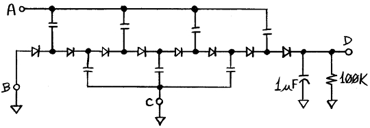
I have used charge pumps for up to 8 or 10 watts. Sometimes it's not very efficient, but it may be
worth it anyway. Here's a circuit I breadboarded recently to get -9V from +5V. This circuit puts out over -19V with a very light load,
but I put the output through an LM337T adjustable negative linear regulator set to put out -9V at up to -200mA from this.
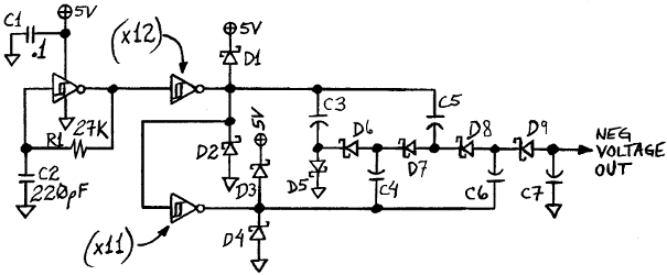
Notes:
The reason for the '14 instead of the '04 is that the oscillator needs to be Schmitt-trigger. The reason for the 74AC (instead of 74HC) is that AC has a much stronger output. Even 74ABT is not significantly stronger for this one, and 74ABT cannot pull up to 5V like 74AC can anyway, which is a big disadvantage.
There are lots of ways to do the above, and I can't cover them all; so if you have an idea for a different one, about all I can say is to breadboard it and try it to see if you can get the needed voltage and current from it. If you want my opinion on a circuit idea, you can email me at wilsonminesBdslextremeBcom (replacing the B's with @ and .).
For other needs of doubling or negating a voltage, sometimes the
7660-related 8-pin DIP ICs are
appropriate. These are capacitive charge pumps. There are many variations, each with their own strength; for example, some have a
higher maximum operating voltage, some have higher operating current, and some even have regulators built in. See the data sheets for the
various operating modes. Ones I have tried are (with a brief description of the part and a few actual numbers from my own experience with
it) are:
Switching regulators (which use inductors), whether buck or boost, are typically a better way than charge pumps to do power
supplies, due to efficiency, particularly when regulation is needed; but they tend to do poorly on breadboards, and their PC-board
layout is not for beginners. (The one I've used most in our commercial products is the
MAX732 which allows you to start with
anywhere from 4V to 9.3V input and get 12V out. Another is the
MAX669 which let us start with a pair
of AA batteries and get 12V out.) One way around the difficulty that switching regulators present for the hobbyist is to use
integrated switching regulators which put all the difficult stuff in a small pre-made module, sometimes with the same pinout as the
popular 7805 for example. I've used the Power Trends 78SR112 and 78ST105 three-pin 12V and 5V switching regulator modules in
prducts. They worked great but unfortunately TI took over Power Trends and discontinued these.
Pololu Robotics and Electronics,
MicroPower Direct, and
Traco Power are three other suppliers of switching-regulator modules.
< I realize now I should add a circuit for a complete modem for storing data and programs on tape, since even at this late
date (2022), we still frequently see interest on the forum. Although tape is pretty much gone, people are using their cell
phones and other digital devices to record audio. >
workbench equip <--Previous
last updated Oct 16, 2023